Figure
1.
Structure of IGBT module
| Citation: |
Wei Huang, Zhiwen Chen. Review on failure analysis of interconnections in power devices[J]. CHINA WELDING, 2022, 31(1): 6-14. DOI: 10.12073/j.cw.20211227001

|
With the wide application of power electronic devices in new energy equipment, rail transit, smart grid, aerospace, electric vehicles and other industries, people and countries put forward higher and higher requirements for their operation reliability and safety. The working environment of power electronic devices in these fields is mostly harsh. For example, they need to withstand extremely high temperature or low temperature and long-term service. These harsh conditions pose great challenges to the reliability of power devices. According toan industrial reports, about 38% of the power converter system faults were caused by the failure of power devices[1]. Furthermore,most of these failure cases of power electronic devices are caused by the failure of interconnection. On the one hand, the interconnections play the role of providing mechanical support and accelerating heat dissipation for chips or components in power devices. On the other hand, it can realize the electrical interconnection between modules. Reliable and stable performance of a power module depends on the reliable connection provided by interconnections.
Power electronic devices are constantly under the influence of temperature change, vibration, shock and corrosion when they operate in harsh environment for a long time[2]. The interconnection produces small defects under the action of these factors. The long-term accumulation of defects will threaten the reliability of the bonding lead and solder layer, such as the fracture and falling off of the bonding lead, and the cracks in the solder layer, leading to shorter service life of the device.
For a power electronic device, the factors affecting the reliability of interconnection are complex, including temperature, humidity, impact, vibration and current etc. In most cases, interconnection failure in power device is a result of various environmental factors. The failure mode of the device needs to be investigated and the location of failure can be located by analysis technologies such as X-ray, ultrasonic microscopy, infrared thermal imaging and dye penetrant. In order to explore the mechanism of interconnection failure, failure analysis technique is vital to unveil the cause and mechanisms.
Temperature is an important factor affecting the interconnection reliability of power electronic devices. The interconnection reliability of power electronic devices is closely related to its service temperature. According to research, the failure rate of microelectronic products increases exponentially with the increase of temperature. For every 10 ℃ increasing in the working temperature of microelectronic products, the failure rate will double. These type of failure for interconnection structure is mainly due to long-term service environment with drastic temperature change in power packaging. It can lead to the gradual deterioration of microstructure in interconnections. The main mechanism of thermal fatigue is the periodic stress in interconnections of power electronic devices due to temperature cycles during the service lifespan of power modules. The accumulation of plastic strain under shear stress will finally lead to the damage of interconnection structure. Thus,the power device fails.
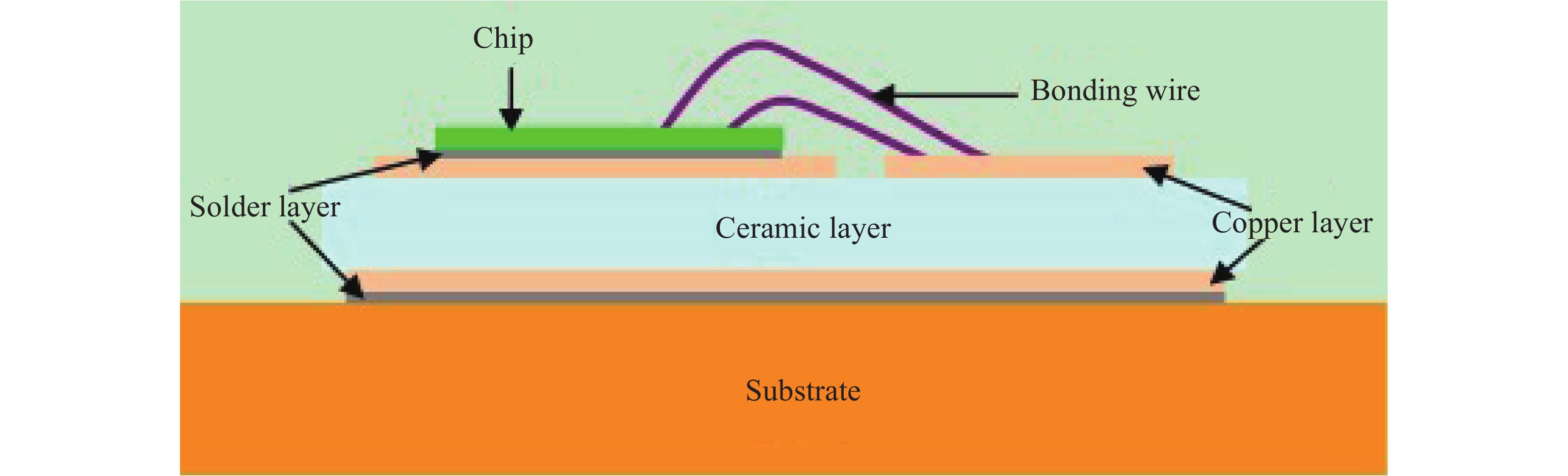
As shown in Fig. 1, it is a typical structure of a power device IGBT module, which mainly includes chip, bonding wire, DBC substrate, solder layer and copper substrate. The thermal parameters of each part of the material are shown in Table 1[3], and it can be seen that the thermal parameters of each layer of materials are very different. The difference in thermal conductivity makes the internal heat distribution of the IGBT module uneven when the power device is working. The difference in specific heat capacity makes the temperature difference of each layer of material very large, and the difference in CTE makes each layer of material produce different degrees of strain. In turn, longitudinal shear mechanical stress is generated between the layers of material. When the power device is in cyclic service, the materials of each layer of the IGBT module suffer from fatigue and aging due to the continuous cyclic stress. Defects such as holes and cracks in the module gradually initiate and expand, and eventually the power device fails due to thermal fatigue. Thermal fatigue failure of power devices can be divided into two types, failure of bonding wire and solder layer.
| Materials | Thermal conductivity k/(W·m−1·K−1) | Specific heat capacity c/(J·kg−1·K−1) | CTE α/(10−6·K−1) |
| Chip(Si) | 148 | 703 | 4.2 |
| Bonding wire(Al) | 237 | 880 | 23.2 |
| Solder layer(SnAgCu) | 50 | 227 | 23.0 |
| Copper layer(Cu) | 397 | 1386 | 17.5 |
| Ceramic layer(Al2O3) | 32 | 780 | 7.7 |
| Substrate(AlSiC) | 185 | 240 | 7.9 |
 DownLoad:
CSV
DownLoad:
CSV
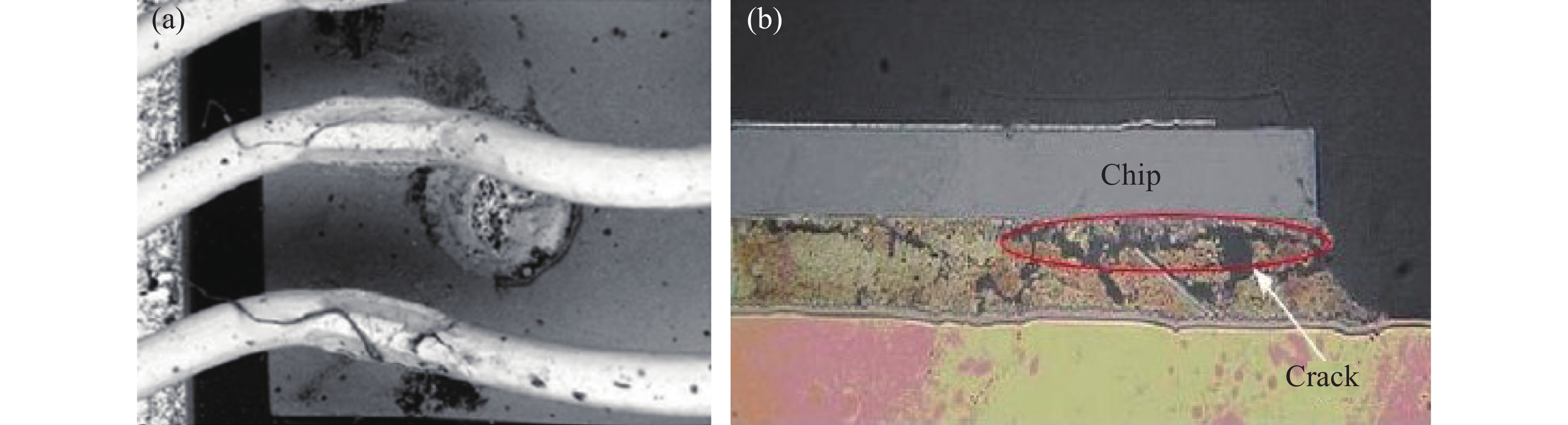
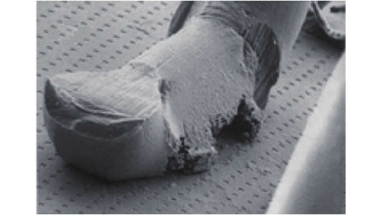
In Fig. 2 a[4], bonding wires peeled off under the accumulation of thermal fatigue, leading to the failure of power devices. Due to the large difference in CTE of the bonding wire and chip materials and the temperature fluctuations at the connection between the two, thermal stress occurs at the connection between the bonding wire and the chip. The continuous action of thermal stress leads to corresponding strain at the joint, and the strain ε caused by thermal stress at the joint can be described as
|
ε=L(αAl−αSi)ΔT
|
(1) |
|
σ=αEΔTj
|
(2) |
where α is the CTE of the material; E is the elastic modulus. When the power device is in operation, the temperature of the solder layer of the IGBT will undergo corresponding cyclic changes, thereby generating alternating cyclic stress and thus cyclic strain. Under the action of long-term cyclic strain, the solder layer is prone to cracks, resulting in thermal fatigue failure of power devices. The lifetime of the IGBT solder layer can be predicted by the Coffin-Manson lifetime model[10]:
|
Nf=B(ΔTj)−aeEakTm
|
(3) |
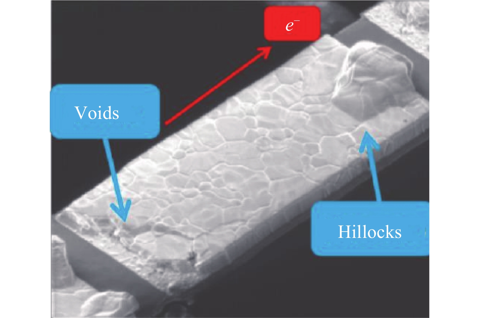
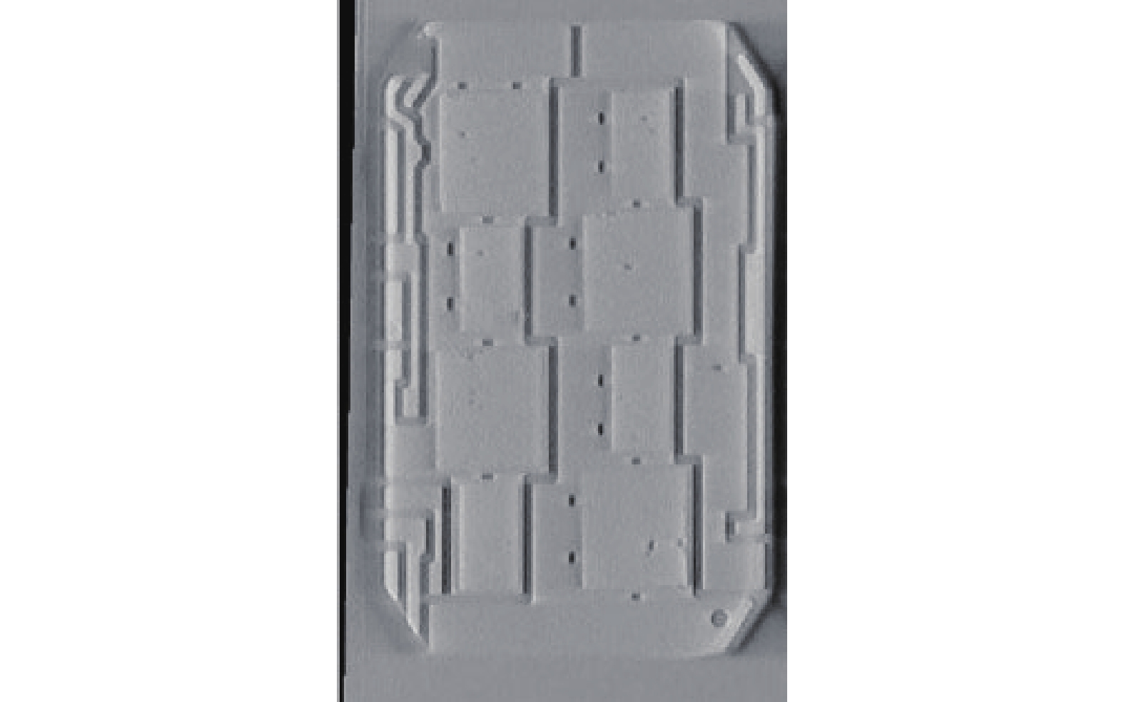
With the development of power electronic devices towards higher power density, the current density also increased significantly. And the current density through interconnections can reach or even exceed 108 A/m2, leading to failure by electromigration[11], as shown in Fig. 3[12].
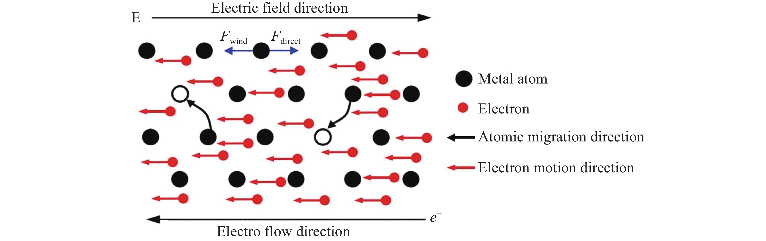
Electromigration is a result of directional migration of metal atoms along the direction of electron movement when high current density passing through. Agarwal et al[13] reported that the current density threshold of electromigration behavior of solder is 103−104 A/cm2. The failure of solder joint caused by electromigration has become an important factor in the failure of power electronic devices. For the mechanisms of electromigration failure, there are two possible factors that can contribute tothe atomic migration in interconnections under high current density. One is electrostatic force Fdirect, also known as Coulomb force, which is from anode to cathode. The other is electron wind Fwind, which is the energy exchange due to the collision between free electrons and metal ions. The atoms are then pushed and migrated along the direction of electron flow[14], from cathode to anode. Fig. 4 illustrates electromigration force[15]. The electrostatic field force and the electron wind force on the metal atoms are equivalent to an average force, namely the electromigration force[16]. It can be expressed as
|
Fem=Fdirect+Fwind=Z∗eρj
|
(4) |
where Z* is the effective charge number; e is the electron charge; ρ is the resistivity; j is the current density.
Generally, for metals, the effect of electronic wind force is stronger than that of electric field force in the electromigration process. Therefore, the movement direction of metal atoms is consistent with that of electronic wind force, from cathodeto anode. The metal atoms of the cathode continuously move towards the anode under the action of electromigration force. Therefore, electromigration will lead to phase segregation, Kirkendall voids, whisker extrusion and polarization effect in the interconnections.
Electromigration Median Time to Failure, (MTF) is generally used in the electronics industry to describe failures caused by electromigration. The median failure time refers to the time it takes for 50% of the interconnecting leads to fail under the same DC current condition, and the failure criterion is that the lead resistance increases by 100%. The electromigration lifetime model is described as[17]
|
MTF=Aj−neEakT
|
(5) |
where A is a constant related to the material; j is the current density; n is the current density index; Ea is the diffusion activation energy; k is the Boltzmann constant; T is the absolute temperature. The MTF is closely related to the current density j and the temperature T. The higher the current density and the higher the temperature, the smaller the MTF and the more likely electromigration failure occurs.
Mechanical stress refers to the stress generated by the interaction between various parts when subjected to external force. The interconnections in power electronic devicesisvulnerable to bending stress, assembly stress and stress caused by vibration and impact. When the stress exceeds the strength of interconnections, it will lead to the cracking and failure of solder layer. Li et al.[18] summarized the failure of interconnections caused by external forces such as vibration and impact during the service of power electronic devices. Based on these failures, some process measures to avoid mechanical stress cracking of solder joints of power electronic devices are proposed in terms of structure design and packaging form. According to the research, 90% of the mechanical and electrical failures can be attributed to fatigueload[19]. When subjected to alternating and periodic stress far lower than their mechanical strength, plastic deformation can be produced and accumulated within interconnections. Dislocations will pile up and link continuously in the process of fatigue deformation. The integrity of crystal will then be destroyed and microcracks will be generated. With the propagation of microcracks, the solder joints and solder layer will fracture and fail.
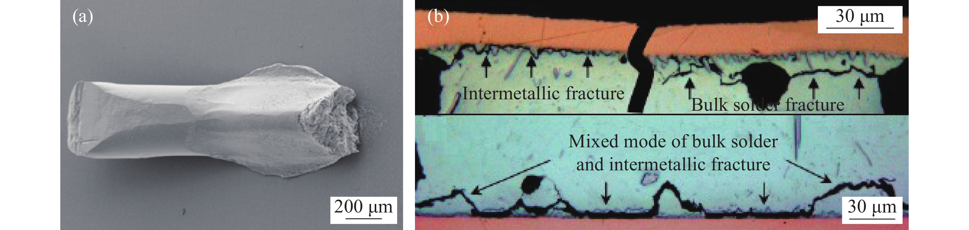
When power electronics are under vibration or force during service, the wire bonding and solder layers are prone to mechanical fatigue and failure. The service life of wire bonding is closely related to its process parameters. Zerny B C et al.[20] studied the effects of loop height, bonding distance and wire angle of the bonding lines on the life of bonding points under vibration loads with a constant displacement amplitude. The results showed that the interaction of height and bonding angle have the most significant impact on its service life, and the main failure mechanism is bonding wire fracture as shown in Fig. 5 a[20].
Fig. 5 b[21] shows the through crack of the solder layer under the action of mechanical vibration. The reliability of solder layers is mainly related to the structural parameters of each interlayers in power devices. Liu et al.[22] studied the effects of substrate thickness, solder layer thickness and substrate size on the service life of joining layers under vibration loads. The results show that the thickness of the substrate has the greatest influence on the solder layers. Reasonably increasing the substrate thickness can effectively improve the service life of the solder layers. The reason is highly likely that the increase in substrate thickness significantly promotes the device quality and improves the seismic performance of the device.
Under the action of external force, the service life of power devices is usually closely related to the fatigue resistance of the material itself. The fatigue resistance of materials is generally expressed by the S-N curve. The S-N curve expression is expressed as
|
c=SbN
|
(6) |
where b and c are constants related to the material; S is the stress amplitude; N is the corresponding fatigue life when the stress amplitude is S. It is obvious that the larger the stress amplitude, the lower the fatigue life of the material.
Under the continuous vibration load, the fatigue damage of the material gradually accumulates. Fatigue failure occurs when the accumulated fatigue damage exceeds the material's bearing limit. Selecting the steinberg model[23] based on Gaussian distribution, according to the S-N curve and the Miner linear fatigue damage accumulation criterion, the vibration fatigue life Eq. (7)[24] and Eq. (8)[25] are obtained.
|
DRV=0.6827fuN1σ+0.2718fuN2σ+0.0455fuN3σ
|
(7) |
|
NRV=1DRV
|
(8) |
Power electronics are ubiquitous in human life, and their service environment is increasingly complex. For instance, power electronics now are more prone to failure due to corrosion, which becomes the main failure cause for power electronics. The dust or water vapor containing acid and alkali can easily adhere to the printed circuit board (PCB) and corrode the interconnection within electronic devices when the ambient humidity is too high. Fig. 6[26] shows the details of a corroded aluminum bond wire. It is widely known that the chemical properties of aluminum are very active and easy to oxidize in air. A dense alumina film will grow on the surface ofaluminum wires. When the humidity of the environment is too high, the alumina film will be converted into an insoluble layer of aluminum hydroxide in water. The property of aluminum hydroxide is amphoteric, which can dissolve in both strong acid and alkaline bases. Afterwards, the surface of pure aluminum can be exposed to form an electrolytic cell or primary cell and to further erode bonding wires. After a long-term chemical or electrochemical corrosion on power electronics, aluminum bonding wires are easy to break, leading to device failure[3].
After determining the failure location and failure mode of power electronics, the failure mechanism is required to be fully explored to improve the corresponding production process and the reliability of power electronics. In order to obtain failure information of interconnection structure in a short time, many researchers use methods of environmental experiment to apply loads including temperature cycle, humidity cycle, electrical load, vibration or impact to the interconnections to simulate the temperature change, humidity change, current change and external force impact unactualservice. At present, the experimental methods based on the reliability of electronic product interconnection under the action of environmental loads mainly include constant temperature and humidity, temperature or humidity cycle, cold and heat shock, high temperature cooking, random vibration, drop, salt spray and aging experiments[27-30].
In fact, the real service environment of power electronics is more complicated. The interconnections are often subjected to enormous environmental loads at the same time. The above experimental methods cannot reliably simulate real service environment of power electronics. Therefore, the influence of multi physical field coupling such as force, heat and electricity on interconnectionreliability has become a research hotspot. Moreover, damage effects of coupling loads on interconnections are not equal to the simple addition of multiple single loads. The interaction between different loads will produce complex coupling effects on the damage process of interconnections. Thus, the coupled field problem is a complex system engineering. Many researchers only have carried experiments in specific coupling environment and no qualitative conclusion on coupling effects on interconnection reliability have been given.
Reliability test is for measurement, verification or improvement of the power device reliability. China and other countries have already formulated relevant standards to standardize the judgment of device reliability in various industries. The relevant standards of China include national standards and national military standards, such as semiconductor discrete device test method GJB 128, electronic component test method GJB 360, electronic component failure rate test method GB/T 1772, etc. MIL standard of United State American is considered as one of the most advanced standards in the world. IEC standards and ISO standards are commonly used international quality and reliability standards. Countries often take international standards as the benchmark during formulating standards. British Standards Association and Japanese national standards issued BS standards and JIS standards, respectively. In the above standards, the applicable scope, test instruments, test conditions and criteria for relevant reliability tests of electronic products are specified. These standards are conducive to the standardization of reliability testing and evaluation of electronic devices.
With the development of microscopic characterizationtechnology, the failure detection methods of interconnections are becoming more diversified. The failure analysis of interconnection structure can be divided into detection technology analysis and condition monitoring analysis. Regarding whether to destroy the overall structure of the power electronic device as a distinction, the detection technology can be divided into non-destructive testing and destructive testing[31].
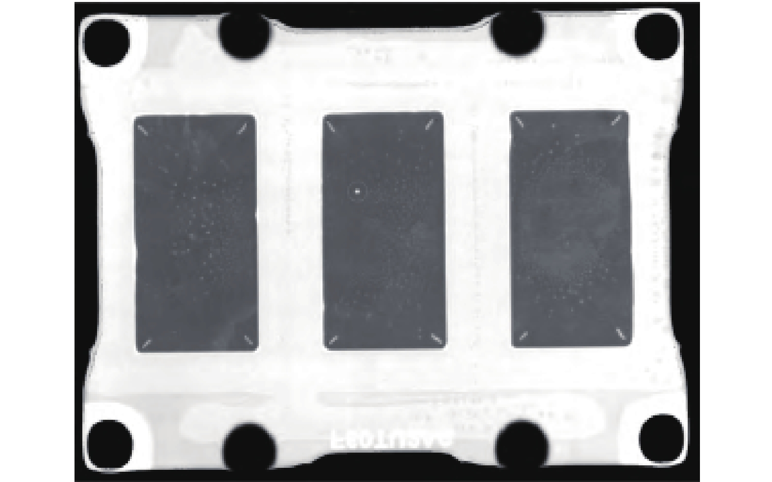
Nondestructive testing technology mainly includes optical microscopy, electron microscopy, X-ray, ultrasonicmicroscopy, laserholographic interferometry and infrared thermal imaging testing technology. The failure analysis and detection of power electronics should first be checked with eyes or a simple magnifying glass. Most device failures cannot be observed with naked eyes. So microscopic observation technologies such as optical microscope or electron microscope can be used to assist detections. As shown in Fig. 7, X-ray testing can clearly detect the hidden defects at the bottom of devices by X-ray transmission characteristics[32]. Ultrasonic will have total reflection at the interface defects and display as white dots[33]. As shown in Fig. 8, ultrasonic micro detection is convenient to intuitively understand the internal structure of devices, which can accurately judge the location, shape and defect size. Chi D Z et al. binarized the ultrasonic D-scan image based on KSW 2D entropy image segmentation method. It enables automatic identification of tiny defects in ultrasound images[34]. Laser holographic interference detection can measure the three-dimensional weldment surface with arbitrary shape and surface condition, obtaining the annular interference fringe or distorted displacement field distribution diagram of the interference fringe at the weldment crack point. Moreover, it can accurately detect the position of the crack point with the acoustic emission monitoring system. Infrared imaging detection technology uses the characteristic of abnormal resistance at the defect location to judge the defect location according to the temperature difference in the thermal image.
Destructive testing techniques mainly include metallographic detection and dye penetrant detection. Dye penetrant detectionis to make high permeability and coloring dyes penetrate into cracked area, and then destroy the interconnection structure. The failure information is obtained by observing the distribution of dyes in the interconnection structure. Metallographic examination is generally combined with optical microscope, scanning electron microscope and dispersive X-ray spectrometer[35]. Generally, after grinding and polishing the sample at the damaged interface, the defect position and interface morphology of interconnections can be observed by optical microscope or scanning electron microscope. Scanning electron microscope with EBSD probe can alsoobtain the orientation information of interface. And dispersive X-ray spectrometer can obtain the composition information of micro region.
This paper reviews the failure mode and mechanism of interconnection failure from following aspects, including thermal stress, mechanical stress, electromigration and corrosion. Major reliability test technologies and failure analysis technique are also summarized.
(1) Temperature, temperature difference, current density, stress, humidity, corrosion ions, etc. are all important factors that lead to the failure of interconnect structures. Among them, thermal fatigue stress caused by frequent temperature differences is the main factor leading to the failure of the interconnect structure in power devices. After the interconnect structure fails, it can be tested for destructiveness or non-destructiveness according to the specific working conditions. Reliability testing can predict the lifetime of power devices. In addition, the online health state detection of power devices can effectively evaluate the aging of the devices, thereby improving the reliability of the entire system.
(2) The failure of the interconnect structure is usually the result of a combination of factors. And the combined effect of multiple factors is not a simple addition of individual factors. In power devices, the temperature field, current field, and stress field are interconnected through coupled variables, forming complex and nonlinear multi-physics coupling problems. Therefore, it is necessary to fully consider the influence of coupling variables between fields in multiphysics modelingin order to explore the failure mechanism of interconnected structures.
| [1] |
Yang S, Bryant A, Mawby P, et al. An industry-based surveyof reliability in power electronic converters. IEEE Transactions onIndustry Applications, 2011, 47(3):1441 − 1451. doi: 10.1109/TIA.2011.2124436
|
| [2] |
Vianco P T, Feng Y. Electronic packaging: solder mounting technologies. Reference Module in Material Science and Materials Engineering. Elsevier, 2016.
|
| [3] |
Mauro Ciappa. Selected failure mechanisms of modern power modules. Microelectronics Reliability, 2002, 42:653 − 667. doi: 10.1016/S0026-2714(02)00042-2
|
| [4] |
Huang S S. Screening technology for aerospace critical power electronic devices IGBT. University of Electronic Science and Technology, 2018.
|
| [5] |
Zhang Y J, Fan H X, Zhang X K, et al. Fatigue life analysis of IGBT module solder layer for VSC-HVDC valve. High Voltage Engineering, 2020, 46(10):3381 − 3389.
|
| [6] |
Li Y, Hou T, He Z P, et al. Power cycle simulation method of press-pack IGBT module basedon semi-direct coupling. Southern Power System Technology, 2021, 15(6):1 − 6.
|
| [7] |
Li Z G, Zhang Y L, Mei S. Research on IGBT thermal resistance degenetate model under temperature recycle. Microelectronic Technology, 2016, 42(2):25 − 31.
|
| [8] |
Zhang J, Qiu Z J, Wang L, Ning P Q. Comparison and Analysis of Power Cycling and Thermal Cycling Lifetime of Power Semiconductor Modules for Vehicles. ELECTRIC POWER, 2019, 52(9):54 − 60.
|
| [9] |
Mc Pherson J M. Reliability physics and engineering: Time-to-failure modeling. New York: Springer, 2010.
|
| [10] |
Hu B, Gonzolez J O, Ran L, et al. Failure and reliability analysis of a SiC power module based on stress comparison to a Si device. IEEE Transactions on device and materials reliability, 2017, 17(4):727 − 737. doi: 10.1109/TDMR.2017.2766692
|
| [11] |
Tu K N, Gusak A M, Li M. Physics and materials challenges for lead-free solders. Journal of Applied Physics, 2003, 93(3):1335 − 1353. doi: 10.1063/1.1517165
|
| [12] |
Ma Rui. Electromigration reliability study of white light CSP-LED. Beijing University of Technology, 2018.
|
| [13] |
Agarwal R, Ou S E, Tu K N. Electromigration and critical product in eutectic SnPb solder lines at 100 degrees C. Journal of Applied Physics, 2006, 100(2):024909 − 5. doi: 10.1063/1.2216487
|
| [14] |
Gupta Raju P A. The electron wind force in electromigration. Journal of Physics and Chemistry of Solids, 1986, 47(11):1057 − 1066. doi: 10.1016/0022-3697(86)90072-7
|
| [15] |
Zhang Y X. Electromigration failure analysis and numerical simulation of metal micro-interconnects under the multi-physical field. Zhejiang University of Technology, 2011.
|
| [16] |
Huntington H B, Grone A R. Current-induced marker motion in gold wires. Journal of Physics and Chemistry of Solids, 1961, 20(1):76 − 87.
|
| [17] |
Black J R. Physics of Electromigraion. Proc of the IEEE Int Reliability Physics Symp. 1983, 142−149.
|
| [18] |
Li F Y, Jiang Q L Wang Y Q, et al. Case analysis of solder joint cracking failure of high-density circuit components of high-reliability electronic products. 2020 China high end SMT Academic Conference, Xi'an, China, 2020, 216 − 222.
|
| [19] |
Zhai D J. Failure mechanism of the interface between ball grid array solder and Cu substrate induced by thermal/current/vibration loading. Chongqing: Chongqing University, 2014.
|
| [20] |
Czerny B, Paul I, Khatibi G, et al. Influence of wirebond shape on its lifetime with application to frame connections. 14th International Conference on Thermal, Mechanical and Multi-Physics Simulation and Experiments in Microelectronics and Microsystems, Wroclaw, Poland, 2013, 1 − 5.
|
| [21] |
Marjamaki P, Mattila T T, Kivilahti J K. A comparative study of the failure mechanisms encountered in drop and large amplitude vibration tests. 56th Electronic Components and Technology Conference, San Diego, CA, 2006, 95 − 101.
|
| [22] |
Liu D J, Wang S M, Wang H J, et al. De sign optimization and vibration performance of IGBT power devices. Electronic Components and Materials, 2020, 39(No.11):91 − 95.
|
| [23] |
Steinberg D S. Vibration analysis for electronic equipment. 2nd ed. New York:John Wiley & Sons, 1988, 137 − 154.
|
| [24] |
Zhang Y, Wang W M, Zhang Y. Research on high cycle fatigue life assessment method of IGBT under electro-thermal-solid coupling. Electronic Components and Materials, 2021, 40(11):1151 − 1158.
|
| [25] |
Yi Z W. Life prediction of PCB under thermal cycling and random vibration loading condition. Electronic Components and Materials, 2019, 38(1):89 − 96.
|
| [26] |
Choi U M, Joergensen S, Blaabjerg F. Advanced accelerated power cycling test for reliability investigation of power device modules. IEEE Transactions on Power Electronics, 2016, 31(12):8371 − 8386.
|
| [27] |
Honarvar S, Nourani A, Karimi M. Effect of thermal treatment on fracture behavior of solder joints at various strain rates: Comparison of cyclic and constant temperature. Engineering Failure Analysis, 2021, 128(8):105636.
|
| [28] |
Jeong Haksan, Min Kyungdeuk, Lee Choong-jae, et al. Mechanical reliability of Cu cored solder ball in flip chip package under thermal shock test. Microelectronics Reliability, 2020, 112:113918. doi: 10.1016/j.microrel.2020.113918
|
| [29] |
Li M L, Gao L L, Zhang L, et al. Interfacial evolution of pure Sn solder bearing silicon carbide nanowires under isothermal aging and thermal cycling. Journal of Materials Research and Technology, 2021, 15:3974 − 3982. doi: 10.1016/j.jmrt.2021.10.022
|
| [30] |
Branch Kelly Marion, Kirubanandham Antony, Chawla Nikhilesh. Mechanisms of thermal cycling damage in polycrystalline Sn-rich solder joints. Materials Science & Engineering:A, 2020, 771:138614.
|
| [31] |
Huang J Y, Cao Y, Gao C. Fatigue failure of microelectronic packaging solder joints: a review. Electronic Components & Materials, 2020, 39(10):11 − 16,24.
|
| [32] |
Ma Y S, Zhang Z. Rapid detection technology of planar CT and its application in electronic industry. Proceedings of 2020 China high end SMT Academic Conference, 2020, 228 − 231.
|
| [33] |
Wang B, Wang Z Z, Chen S, et al. Application of acoustic inspection in evaluation of IGBT reliability. Electronic Components and Materials, 2018, 37(6):89 − 92.
|
| [34] |
Coquery G, Lallemand R. Failure criteria for long term accelerated power cycling test linked to electrical turn off SOA on IGBT module. Microelectronics Reliability, 2000, 40(8):1665 − 1670.
|
| [35] |
Chi D Z, Gang T. Defect detection method based on 2D entropy image segmentation. China Welding, 2020, 29(1):45−49.
|
| [36] |
Mo S X, Dong S K, Zhu H, et al. Corrosion behavior of aluminum/steel dissimilar metals friction stir welding joint. China Welding, 2021, 30(3):20−30.
|
| 1. | [No author name available]. Research progress in high-performance power device packaging and power cycle reliability | [高性能功率器件封装及其功率循环可靠性研究进展]. Hanjie Xuebao/Transactions of the China Welding Institution, 2023, 44(12): 124-136. DOI:10.12073/j.hjxb.20230613015 | |
| 2. | [No author name available]. Application and reliability of Au-Sn electroplated layer on the CSP hermetical packaging | [金锡镀层在 CSP 气密封装中的应用及其可靠性]. Hanjie Xuebao/Transactions of the China Welding Institution, 2023, 44(12): 49-55. DOI:10.12073/j.hjxb.20230613003 |
Website Copyright:© Editorial Office of China Welding
黑ICP备09092524号-3
Editor Office: 2077 Chuangxin Road, Harbin 150028,P.R.China
E-mail: cw@hwi.com.cn
Tel: +86-451-86323218

| Materials | Thermal conductivity k/(W·m−1·K−1) | Specific heat capacity c/(J·kg−1·K−1) | CTE α/(10−6·K−1) |
| Chip(Si) | 148 | 703 | 4.2 |
| Bonding wire(Al) | 237 | 880 | 23.2 |
| Solder layer(SnAgCu) | 50 | 227 | 23.0 |
| Copper layer(Cu) | 397 | 1386 | 17.5 |
| Ceramic layer(Al2O3) | 32 | 780 | 7.7 |
| Substrate(AlSiC) | 185 | 240 | 7.9 |
DownLoad:
CSV